Results on commercial cells, validated by a national lab.
This is a real cell hiding real lithium plating.
Every other test on the line called it healthy.
One result is a demonstration.
Six is a track record.
Across four years, four defect classes, and partners from LG to a national lab — every detection below is tied to a specific commercial cell and program milestone.
Torn-tab detection
Detected submillimeter torn tabs in 59 Ah GM Bolt-type cells for LG during Phase I — the exact defect class behind the $2B recall.
Lithium-plating detection, independently validated
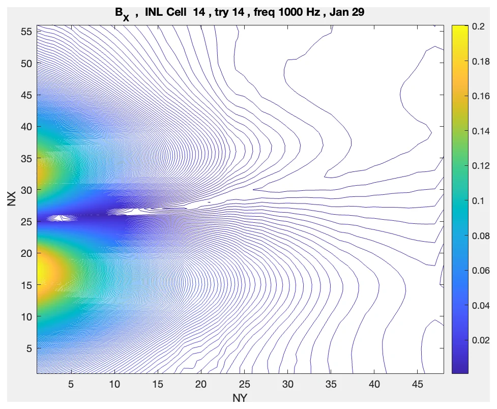
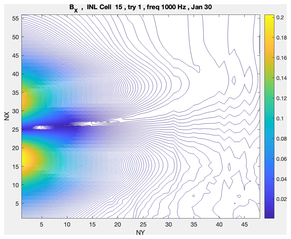
Detected plating in 11 Ah commercial Kokam cells, validated with Idaho National Laboratory — to our knowledge a first for any non-invasive sensing method. The measured data is Figure 3, above.
Hidden weld-defect localization
Localized a hidden weld defect in 30 Ah commercial pouch cells returned from the field — a cell that had passed conventional QC. (2025)
Format- and chemistry-agnostic in practice
Demonstrated across NMC pouch and LFP prismatic formats, from 200 mAh to 100 Ah class cells — four distinct defect groups to date. (2025)
Phase IIB Go/No-Go: passed
EMIS output correlated with fast-charge cycle number in 9 of 10 cells (each ≥10 Ah) — the DOE-defined success threshold for autonomous, machine-readable detection. (2025)
Instrument-grade precision, commodity cost
0.02% impedance accuracy (0.005 mΩ at 2.5 mΩ) on in-house electronics, while hardware cost fell $50k → $4k → ~$1k across program phases.
Send us your cells. We send back the maps — your defects, your data, in two weeks.
Start a validation project →What the lab measured once, EMIS reads in every defect class.
The same physics that resolved the INL plating signature generalizes: a torn tab pulls the field toward a corner, plating blooms as a hot-spot, a short collapses the contours to a point. Each break in symmetry is distinct — and machine-classifiable.
Anyone can build an instrument. We're building the reference.
That measured result is proof of one cell. The deeper advantage is what happens when you measure thousands: every image EMIS captures sharpens a model trained on real, validated commercial-cell signatures — the layer the industry will calibrate against.
Here's how a single measurement compounds into a standard a competitor can't simply buy:
Scan
EMIS images a cell's internal current density on the line or the bench — on-prem, your data never leaving the factory.
Label
Each signature is tied to a known outcome — torn tab, plating, short, weld defect — validated against teardown and national-lab ground truth.
Sharpen
The model that turns a 2D field into a machine-readable verdict improves — better thresholds, fewer false positives, broader cell coverage.
Compound
Detection improves for the whole field, which pulls more cells through EMIS. The reference standard for "is this cell electrochemically sound" accrues to whoever measured the most cells first.
For investors: the instrument is the wedge; the labeled-signature dataset and the on-prem inference standard are the moat. Earlier patent priority (2013) plus the first large corpus of measured commercial-cell signatures is a position a better-funded fast-follower cannot simply buy.
A single point of scrap costs a gigafactory roughly €10M a year.
The battery industry still lacks the inline QC maturity of semiconductors. A chip fab inspects every wafer in real time; most cell lines rely on delayed testing and days of aging — and still miss the defects that matter most.
Large-cell scrap runs double small-cell cost because manufacturers raise thresholds to cover what they can't measure. EMIS halves it — against a software fee comparable to existing QC.
Every fast tool on the line reads one of two signals. EMIS reads a third.
Each waits for damage to surface as voltage, gas, or geometry. EMIS images the current density itself — where the recall-class defects appear first.
| Self-discharge | Ultrasound | X-ray / CT | Eddy current | Parthian EMIS | |
|---|---|---|---|---|---|
| Signal measured | Self-discharge current | Acoustic interfaces | X-ray attenuation (geometry) | Surface-induced currents | Internal current density |
| Images electrochemical function | Bulk average only | No | No — structure only | No | Yes — spatially resolved |
| Catches torn / misaligned tabs | No — until leaking | Limited | If geometric | Surface only | Yes — demonstrated |
| Catches lithium plating | No | Only after drying/gassing | No | No | Yes — INL-validated |
| Catches resistive weld defects | No | No | Geometry, not resistance | Limited | Yes — demonstrated |
| Needs cell relaxation / aging | Yes | Built + wetted first | No | No | No |
| Works before electrolyte injection | No | No | Yes | Shallow layers | Yes |
| Output | Pass / fail | 2D map / scalar | 3D geometry | Scalar | 2D map today → scalar (roadmap) |
Flags defects on a dry electrode stack — before electrolyte injection, with no relaxation period.
Catches the recall-class faults the fast tools can't see — torn tabs, shorts, and lithium plating, validated.
Rides the existing ACIR station — no added line time, a <1 mm sensor plate, ML on-prem.
An MRI for the inside of a cell — no contact, no opening it up.
A cell's own current makes a magnetic field. Read that field from just above the surface, reconstruct the current inside, and a defect reveals itself as broken symmetry. Here's the idea on a chalkboard.
The Inhomogeneity Mapper, for research labs.
Teams studying lithium plating and fast-charge cell design get an imaging tool that sees what nothing else can — today. Up to 1,000,000× more data points per cell than a single ACIR reading.
A benchtop gantry images a cell's internal current density — non-contact, no teardown — and returns a machine-readable defect map. Chemistry-, size-, and format-agnostic, 200 mAh to 100 Ah. From US$ 9,975 / 6-month rental.
Get the datasheet
Full EMIS08S01 specifications, measurement modes, and channel architecture — everything your engineers need to evaluate fit.
Run a validation
Send us cells — healthy, suspect, or returned from the field. We image them and send back the current-density maps with a defect read. Your data, in about two weeks.
Rent the instrument
The EMIS08S01 on your bench. License, EIS hardware, and the 8-channel mapper included; XYZ gantry optional.
Pricing shown for the research configuration. Manufacturing / inline integration is scoped directly — talk to us.
Invented by its founders. Vetted by the people who built the field.
Farshid Roumi, PhD
Caltech PhD. Inventor on 23+ patents. Recognized by the U.S. government as an Individual with Extraordinary Ability in Science.
Full bio
Former senior research scientist at Caltech, where he founded and led an advanced energy-storage lab. Recognized as an Individual with Extraordinary Ability in Science and Engineering (2012); selected for the National Academy of Engineering's Frontiers of Engineering (2023).
Michelle Mahshid Roumi, PhD
ML and signal processing for faint signals in noise. Her neutrino-detector hardware has run autonomously in Antarctica since 2013.
Full bio
Developed an FPGA image-processing engine up to 4× faster than the reported state of the art. Former Caltech postdoctoral scholar; co-inventor of the EMIS patent family; PI of this program since Phase I.
Co-inventor of the graphite anode in every lithium-ion battery; Draper Prize laureate; co-inventor on 140+ battery patents; former president of the International Battery Association.
Member of the National Academy of Engineering for co-inventing the communications ICs in our cell phones; former Senior Vice President at Broadcom.
Former Executive Vice President at Wells Fargo, where he led the bank's venture investing business and founded its Global CleanTech Group.
Former Johnson Controls executive director for systems electronics and battery management systems; senior roles across EV battery manufacturing and integration.
Tell us about your cells.
Request a validation — or write directly to froumi@parthiannrg.com
We respond within two business days. Your cells and your data stay yours — NDA-backed.
Technology foundation
Invented at Caltech (2013) and exclusively licensed to Parthian, with NAE-member advisors and a published image- and signal-processing track record behind the machine learning.
A substantial issued-and-pending patent family spans US, EU, JP, KR, and CN.
Who we work with
- 01 Gigafactory quality-control & process engineers
- 02 National-lab & university battery researchers
- 03 Strategic partners & investors